Click image to enlarge.
The HP 5370A has some bugs in its firmware which effect GPIB operations. Later versions of the 5370B are reported to have these bugs fixed. It appears that this firmware is compatable with the 5370A. This page documents how to use the 5370B firmware on a 5370A. The 5370B firmware image is found here.
This image is from a unit with date code 2332A (32nd week of 1983), which is a fairly early revision of the 5370B (the 5370A went to 2311A, 11th week of 1983 and the 5370B started at 2316A, 16th week of 1983). The same image was found in a unit with date code 2438A. 5370B revisions went to at least 2904A (4th week of 1989). It is not known if this is the most recent 5370B firmware, and may have bugs of its own, but it does appear to fix some GPIB bugs found in the 5370A.
Here is some information on known 5370 firmware versions:
|
5370A ROM (date code unknown)
# cksum 5370A8K.ROM 3481479018 8192 # md5sum 5370A8K.ROM b07af746a9bd646fdb4f52969b7a5e89 |
5370B ROM from series 2332A
# cksum HP5370B.ROM 1419651446 8192 # md5sum HP5370B.ROM 9ed5d11e77d97c8ff63cf59524027136 |
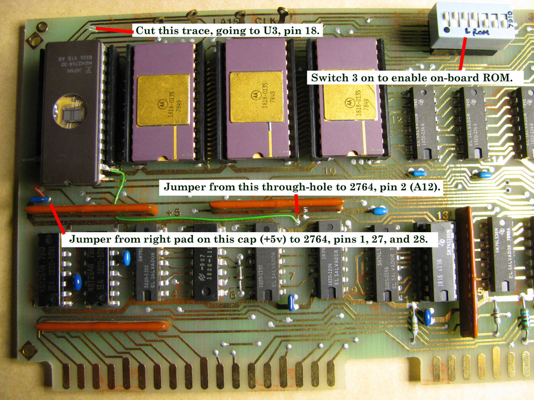
The 5370A CPU board ("A9 Processor Assembly") has a socket at U3, intended to hold a 24 pin ROM. By making some changes to the board, this can be made to accept a larger ROM, able to hold the 8K firmware file. Changes are also needed so that the ROM appears at the correct spot in the address space.
These instructions are based on using a 2764 type EPROM to hold the firmware. Other EPROMs might be wired slightly differently. Note that a 2764 is a 28 pin chip, plugging into a 24 pin socket. 2764 pins 3-14 map to U3 pins 1-12; 2764 pins 15-26 to U3 pins 13-24. Pin numbers given here are referenced to either the socket (U3) or the 2764. Don't mix them up.
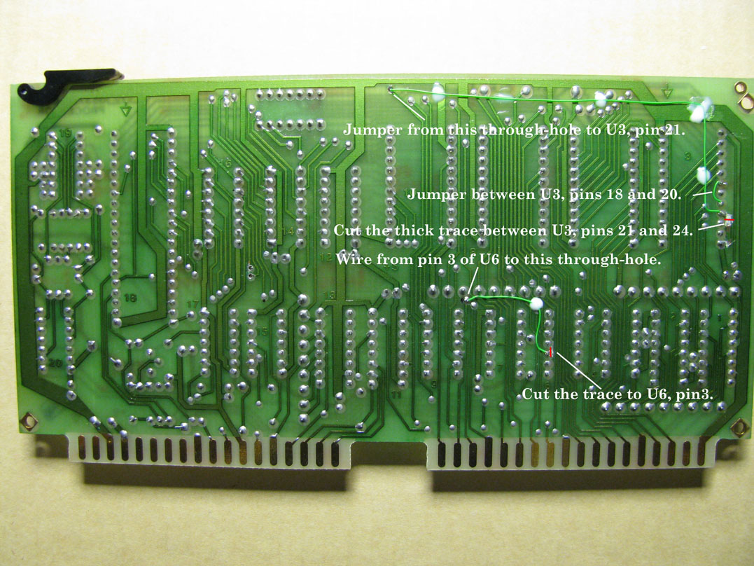
1. Cut the trace going to U6, pin 3.
2. Jumper from U6, pin3 to the through-hole as shown in the image. These changes readdress the ROM socket to the proper address.
3. Cut the thick trace between U3, pins 21 and 24. This removes +5 V from pin 21.
4. Jumper from U3, pin 21 to the through-hole, as shown. This connects to address line 11.
5. Jumper between U3, pins 18 and 20. This connects /OE and /CE (Output Enable and Chip Enable) together on the EPROM.
On the component side of the CPU board, make these changes, as shown in the image below:
5. Cut the trace going to U3, pin 18. This is A11, which we connected elsewhere, in step 4.
6. Install a programmed 2764 in socket U3 (5370B firmware is here), as shown. Note that pin 26 of the 2764 (which would have gone into pin 24 of the socket) is bent outward so it doesn't get connected. Also, pins 1, 2, 27, and 28 will not be in the socket.
7. Connect pin 2 of the 2764 to the through-hole as shown. This is address line 12.
8. Connect pins 1, 27, and 28 of the 2764 together, then to the inboard pad of the nearby bypass capacitor, as shown. This is +5 V.